Comparison of two control methods for unipolar SPWM and zero-crossing output characteristics
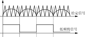
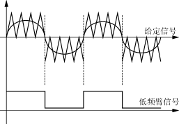
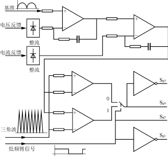
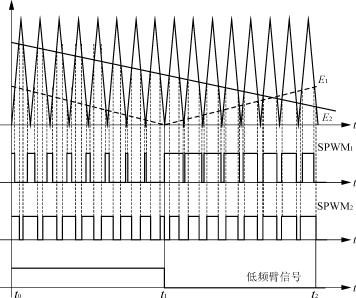
Abstract : For inverters using SPWM, the unipolar inverter method only uses a pair of high-frequency switches, which has the advantages of low loss and less electromagnetic interference compared with bipolar inverters. The generation methods of unilateral and bilateral SPWM in unipolar inverter and their respective control methods are introduced respectively. The oscillation of these two control methods near the zero crossing of sine wave voltage is analyzed. The simulation and circuit test prove bilateral. SPWM mode performance is superior. Keywords : unipolar; sinusoidal pulse width modulation; zero-crossing oscillation 0 Preface With the development of control technology and the continuous improvement of equipment performance requirements, the electrical equipment in many industries is no longer directly connected to the AC grid, but the power is converted by power electronic power, their amplitude, frequency, stability and change. The form is different depending on the electrical equipment. Such as communication power, arc welding power, motor frequency converter, heating power, automotive power, green lighting power, uninterruptible power supply, medical power supply, charger, etc., they use the power to rectify the grid power Obtained after inverter transformation. Therefore, high-quality inverter power has become an important research object of power technology. 1 Working principle 1.1 Main circuit topology and SPWM generation The topology of the unipolar SPWM inverter circuit is shown in Figure 1. It consists of two bridge arms consisting of four switching tubes of the full bridge. One way operates at the high frequency switching operating frequency, called the high frequency arm (S 3 , S 4 ); the other way switches with the output sine wave frequency to become the low frequency arm (S 1 , S 2 ). Figure 1 The main circuit structure of the inverter circuit There are two ways to generate SPWM for unipolar inverters. The first control method is to rectify a given carrier (sine wave) into positive, and the modulated wave (triangle wave) is also positive, as shown in Fig. 2(a), called single-sided SPWM control; the second control method is The given carrier (sine wave) is a complete sine wave. The modulating wave (triangular wave) is positive when the sine wave is positive and negative when the sine wave is negative, as shown in Figure 2(b). Bilateral SPWM control. (a) Both carrier and modulation waves are positive (b) Modulation wave polarity changes with carrier Figure 2 Comparison of two SPWM generation principles The mechanism of the above two control methods for generating SPWM is different, and the respective control circuits are also different. 1.2 Two control methods for unipolar SPWM 1.2.1 Single-sided SPWM control The control circuit of the single-side SPWM is shown in Figure 3. Sg3 and Sg4 in Fig. 3 respectively correspond to the driving signals of the upper and lower tubes of the high frequency arm; Sg1 and Sg2 respectively correspond to the driving signals of the upper and lower tubes of the low frequency arm. Due to the switching action of the low frequency arm, the PWM output properties of the high frequency arm change. For example, the narrow pulse of Sg1 originally corresponds to the output low voltage when the zero crossing occurs, and the low frequency arm suddenly becomes a high voltage after switching. Therefore, PWM has a mutation process. Figure 3 Single-sided SPWM control circuit Figure 4 shows a schematic diagram of the single-sided SPWM control method at zero crossing. In Figure 4, E1 is an error signal that is theoretically in phase with the reference (voltage waveform). Since there is an integral link in the voltage loop and the current loop, the actual output error signal E2 and the reference signal are based on the nature and weight of the load. There is a phase difference. In the figure, SPWM1 is the driving signal of the upper tube of the high-frequency arm, and SPWM2 is the driving signal of the upper tube of the actual high-frequency arm. 1) Time t 0 ~ t 1 As can be seen from Fig. 4, at time t 0 ~ t 1 , since the given low frequency arm signal is 1, corresponding to Fig. 3, it can be known that the low frequency arm of the main circuit is turned on, in Fig. 4 The SPWM corresponds to the drive signal of the upper tube of the high frequency arm, and the SPWM drive signal of the upper tube gradually becomes smaller. It can be seen from Fig. 1 that at the time t 0 to t 1 , the output sine wave signal gradually changes from positive to zero. 2) Time t 1 At time t 1 , the low-frequency arm signal changes from 1 to 0. Therefore, the low-frequency arm is turned on from the lower tube to the upper tube. It can be analyzed from Figure 3, and the low-frequency arm is switched. The SPWM comparator is also switched. Therefore, the SPWM (high-frequency arm upper tube) generated by the E 1 error signal immediately becomes S100 near 100% at time t 1 and then gradually becomes smaller. The driving of the lower arm of the high frequency arm is complementary to the driving of the upper tube of the high frequency arm, so the driving of the lower tube of the high frequency arm gradually becomes larger from zero. It can be seen from Fig. 1 that the output sine wave signal gradually changes from 0 to negative. 3) Time t 1 to t 2 The actual output error signal E 2 will be different from E 1 by one phase. Therefore, the generated SPWM 2 is different from SPWM 1 . As can be seen from Figure 4: after a time t, SPWM 2 0 immediately, since the high-frequency signal is complementary to the tube arm SPWM 2, corresponding to the main circuit, the tube at time t 1 to a high frequency immediately larger arm The duty cycle is turned on, then the duty cycle is gradually reduced (SPWM 2 is gradually larger), the high-frequency arm down-tube signal is not gradually increased from 0, and the sudden change of SPWM will inevitably cause the output sine wave signal to be Oscillation of zero crossings. The solutions available are as follows: (1) At the same time as the low-frequency arm is switched, the output error signal is artificially discharged to be 0, so that the oscillation caused at the zero-crossing point can be attenuated; (2) Artificially advancing or delaying the low-frequency arm signal by a certain phase. However, this scheme is difficult to be accurate because the phase of the low-frequency arm signal is affected by the load and weight. Next page 106cm Pvc Vinyl Wallpaper Vigour New Designs
China leading manufacturer and supplier of 106cm Design Pvc Wallpaper for Project Home Decor Wallpaper
Wallpaper Material: PVC/Vinyl
Wallpaper Size: 1.06*10m, 1.06*15.6m
106Cm Pvc Vinyl Wallpaper,Bedroom Pvc Wallpaper,Morden Design Wallpapers,Living Room Wall Paper SHAOXING VIGOUR DECORATION MATERIAL CO.,LTD , https://www.vigourwallpaper.com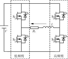
Wallpaper Style: Flowers
Wallpaper Weight: 200 - 550g/sqm