Effect of Corrosion Weight Loss on Lifetime of Silicon Chips
Crystalline silicon solar cells are a major force in the ongoing development of new energy. Crystalline silicon solar cells must undergo surface texture, diffusion, etching, deposition of anti-reflection layers, and screen printing in the production process. The surface texture process includes the removal of the damaged layer of the silicon wafer, surface cleaning, and anti-reflection. The formation of microstructures and other functions are indispensable for battery production. The lifetime of minority children is an important parameter in the design and production of solar cells, reflecting the degree of recombination of solar cells on the surface and the substrate. In order to improve the photoelectric conversion efficiency of solar cells, it is necessary to increase the lifetime of the minority carriers as much as possible and increase the diffusion length of minority carriers. In theory, the longer the minority carrier lifetime, the higher the short-circuit current and the open circuit voltage of the solar cell, and the solar cell's conversion efficiency will be correspondingly improved. Among them, the mechanical damage layer on the surface of the original silicon wafer is the main recombination center of the minority carrier (the minority son) due to the presence of a high concentration of lattice defects, which is the main reason that leads to a low measurement lifetime and battery performance. Measurement of lifetime usually requires surface passivation to reduce the effect of surface recombination. As the cost of battery production continues to drop, the thickness of the wafer continues to decline. In the surface texture process, it is necessary to achieve the purpose of completely removing the damaged layer, and at the same time, to reduce as much as possible to avoid excessive corrosion and create difficulties for subsequent production. Therefore, it is particularly important to determine the minimum corrosion weight loss of the silicon wafer. This article is to use the method of testing the minority son's life to assess the minimum corrosion weight required from the side. It can be seen that using the minority son life test in the process has indeed a certain significance. Experimental program Using the same 6.5' silicon wafer (silicon wafer area 15481mm2), resistivity 1-3Ω · cm, corrosion in the same alkaline texturing solution, take a piece of silicon at regular intervals, measure the corrosion before and after each wafer Weightlessness. The silicon wafer was immersed in 5% HF for 5 min, and the wafer was rinsed with pure water. According to the method of 8.4.2 of GB/T 26068-2010 "Contactless Microwave Reflection Photoconductivity Attenuation Test Method for Silicon Carrier Recombination Lifetime", the silicon wafer after etching is immediately placed in a solution containing iodine. Passivation treatment. A microwave photoconductor decay method was used to test the minority lifetime. The test equipment was the WT-1000 minority son lifetime tester manufactured by Semilab Corporation and the WCT-120 minority son lifetime measurement instrument of Sinton Corporation, USA. The former is a measuring instrument based on microwave reflection photoconductance (MW-PCD) method, which is based on Quasi-steady state Photoconductance (QSSPC). Three pieces of each corrosion weight loss were selected in the experiment, and the minority life was measured on two kinds of machine tables respectively, and the average value was calculated. Fig. 1 Comparison of the centralized minority carrier lifetime measurement technology, corresponding to the typical injection level range of each technology According to the way of carrier generation in semiconductors, the test life has three basic methods: transient photoconductor attenuation (TPcD), steady-state photoconductive attenuation (SSPCD), and quasi-steady state photoconductive (QSSPC). Photoconductivity is an important factor in semiconductor materials. It describes the change of conductance of a material with illumination. There are several ways to use photoconductivity to measure minority lifetimes. All the techniques are contactless. The working principle is that photoexcitation generates excess carriers. These excess carriers generate additional photoconductors based on the dark conductance of the sample. The change of carrier concentration leads to the conductivity of the semiconductor. The change: Here, W is the width of the silicon wafer, and μn and μp are the electron and hole mobility as a function of doping concentration and injection level. These additional time changes in photoconductivity reflect the excess carrier concentration and its short-term behavior, that is, the minority lifetime. Our company manufactures the finest range of Hot Dip Galvanized Ladder Type Cable Trays is suited for heavy weight cables. These cables have the capacity to carry multi network cables without any complication. Our cable trays are accurate in dimensions and have longer life in comparison to other types of cable trays. These are easily assembled and attached to floor, wall, ceiling or top of racks. Hot-Galvanized Ladder Cable Tray Hot-Galvanized Ladder Cable Tray,Hot-Galvanized Cable Tray,Hot-Galvanized Cable Ladder Yangzhong Huaxin Power Equipment Co.,Ltd , http://www.huaxinbusbarchina.com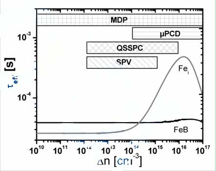
Features :
High tensile strength
Sturdy construction
Dimensional accuracy
Easy to assemble & install
Sturdy built
Corrosion free
Low maintenance
Attach to floor, ceiling, wall or top of rack & cabinets
Available in several widths, heights and lengths
Support large quantity of network cables
Cut & form smooth curved transitions around obstacles
Install quickly using drop in support
Applications
Shopping malls
Hotels
Railways
Airports
Hospitals
Residential complexes
Commercial buildings
Industries
Product Details:
Length 1000/2440/3000/6000 mm
High 50-150 mm
Side Rail Height 50-300 mm
Max. Working Load 1000 KG
Cable Tray Coating Galvanized Coating
Material Steel, Stainless Steel
Tray Type Ladder Type Cable Tray