Hefei Research Institute made series progress in research of porous alumina photonic crystals
Recently, Institute of Solid State Physics, Chinese Academy of Sciences, Hefei Institute of Materials Science has made a series of advances in the research of porous alumina photonic crystals. The concrete manifestations are the interaction between light and matter and the study of their optical properties. The relevant results have been published in the Journal of Materials. Chemistry C, Scientific Reports, Journal of Physics D: Applied Physics, Annalen der Physik, and Nano Research. Photonic crystal is a type of optical material that has a periodic dielectric structure on the optical scale. It is similar to the modulation of the electron wave function of the semiconductor lattice. The photonic crystal can perform the electromagnetic wave of a specific wavelength. Modulation, when the frequency of light falls within the Photonic Band Gap, light propagation will be completely prohibited. Photonic crystals rely entirely on their own structure to achieve light control, which is of great significance in optical devices and future photonic integration. Therefore, studying the interaction between photonic crystal structure, material and photonic bandgap is the basis for applying it to new nanophotonic devices, optical information transmission and optical chips. In recent years, Fei Guangtao of the Hefei Institute of Solids Research Institute has devoted himself to the research of porous alumina photonic crystals. Previously, Wang Qi and others of the research group have obtained series on the preparation of intact photonic crystals and on the characteristics of photonic band gaps. progress. Recently, the research group Shang Guoliang et al. conducted in-depth research on the interaction and optical properties of light and material in porous alumina photonic crystals, and made a series of progresses. The preparation of a photonic crystal with a narrow bandgap and realization of a sensor that relies on the change in refractive index is expected to promote the development of sensing materials. The porous alumina photonic crystal is obtained through the anodized alumina sheet. Under certain anodic oxidation voltage, the alumina pore channel grows periodically in the growth direction and the bifurcated pores form a straight pore layer and bifurcated pores. The periodic structure of the layer, so the porous alumina photonic crystal is a nano-scale periodic porous structure. Although photonic band gaps can be realized in various structures, the narrow photon band gaps are still difficult to achieve. For porous alumina photonic crystals, the bandgap width is usually several tens of nanometers to a few due to the effect of the acidic electrolyte. Between hundred nanometers. They used the compensation voltage mode to overcome the difficulties in the inhomogeneity of the structure before and after the preparation process. A photonic crystal with a narrow bandgap was prepared with a bandgap width of at most a few nanometers. Because of this all-porous porous structure of porous alumina photonic crystals, they used this photonic crystal to successfully implement a simple sensor that relies on refractive index changes (Mater. Lett. 110, 2013, 156-159; J. Mater. Chem. C 1, 2013, 1659-1664; J. Mater. Chem. C 1, 2013, 5285-5291; Chinese J. Chem. Phys. 27, 2014, 121-124). This sensing method is different from the electric signal sensor. When the photonic crystal absorbs the object to be detected, the effective dielectric constant of each layer of the photonic crystal is changed, thereby causing a change in the position of the photonic band gap, and by tracking the change of the position of the photonic band gap. The change in the amount of detected material in the environment can be obtained. If the band gap is in the visible light range, the entire detection method can be completely separated from the electrical signal. Compared with the detection of electrical signals, the detection of optical signals is more safe and reliable, which is expected to be applied to the in-situ detection of flammable, explosive, and electro-degeneration material, making it a promising sensor material. The phenomenon of Fano resonance is observed in porous alumina photonic crystals, and it is helpful to integrate Fano resonance into porous alumina photonic crystals in new optical devices to gain more potential applications. It is well known that the interference fringes appearing in the Young's double-slit experiment have opened a new chapter in optics. Also based on the principle of interference, the interaction between the discrete state and the continuous state discovered by Ugo Fano in 1903 was later called the Fano resonance named after his physical phenomenon, Fano resonance. It is an asymmetrical line pattern after intervention. Fano resonance is a common physical phenomenon, and people have observed the phenomenon of Fano resonance in many fields. However, it is difficult to observe the phenomenon of Fano resonance in photonic crystals. This is mainly due to the fact that the continuous state light scattering in the photonic crystal is not obvious, and the photonic band gap is relatively wide, and the entire photonic crystal does not show typical discrete states. Porous alumina photonic crystals are nanometer-scale periodic pore structures that produce Rayleigh scattering of incident light, while periodic structures also generate strong Bragg scattering for some light, scattering of these two kinds of light. The states will interact within a certain range. Using the narrow bandgap (8 nm at the narrowest point) of Bragg light scattering and the interference of the Rayleigh scattering of light by the porous material, an asymmetrical linear pattern was observed in porous alumina photonic crystals, and The theoretical calculations confirm that this asymmetrical line type is derived from the Fano resonance (Sci. Rep. 2014, 4, 3601), and no previous reports have been found in this material structure system. This finding helps to further understand the interaction of light and matter in porous alumina photonic crystals, since Fano resonance exhibits light transmission from light to light in a narrow wavelength range, making it a very good optical switch. Photonic devices. At the same time, this research has provided assistance for the future in new optical devices that integrate the Fano resonance in porous alumina photonic crystals for more potential applications. Unidirectional optical transmission is achieved, providing a basis for potential applications of direction-dependent photonic devices. Unidirectional light transmission, as the name suggests, means that light can only travel in one direction when passing through an object. Due to the presence of Rayleigh scattering, light loss occurs when light passes through a porous alumina photonic crystal, and the distance travelled by the light is different. This loss will be different. Using this property, they prepared heterostructure photonic crystals and achieved Unidirectional Light Propagation. For light incident from both sides of the sample, the depth of the incoming sample is different, resulting in a different loss of light, so that the color of the sample when viewed from both sides is different. By modulating a variety of photonic crystal combinations, a unidirectional light-transmitting sample with full coverage in the visible light range is achieved (Ann. Phys. DOI: 10.1002/andp.201500286). This provides a simple and feasible method for unidirectional optical transmission, which only requires the introduction of energy loss in the system. Similar to the application of diodes in the field of electricity, photonic crystals with unidirectional light transmission can be applied to direction-dependent photonic devices. Since the unidirectional light transmission shown in the article can be applied to optical unidirectional conduction devices and other potential applications in integrated photonic chips in the future, the article has been subject to the cover article of Ann. Phys. . The capillary condensation and optical properties in porous alumina photonic crystals provide a new possibility for the in-situ detection of light loss mutation transitions. People call a capillary tube with a very fine inner diameter called a "capillary tube," chalk sucks ink, a towel absorbs sweat, and the roots, stems, and leaves of the plant convey nutrients such as capillaries. Capillary condensation is another very important feature of the capillary. It is due to the spatial limitation of the gas molecules in the capillary wall, which increases the interaction between molecules and causes the vapor pressure of the gas-liquid equilibrium in the tube to be lower than in the conventional environment. The vapor pressure reduces the concentration of the substance required for the transition from gas to liquid. In other words, because the capillary tube is very fine, the gas preferentially condenses to form a liquid in the capillary tube. Porous alumina photonic crystals as a nano-scale porous material, which should have the same capillary condensation phenomenon, at the same time, due to the presence of incident light cut-off zone, capillary condensation phenomenon will have an impact on the incident light cut-off zone. They studied a series of optical phenomena caused by capillary condensation of porous alumina photonic crystals in the adsorption of organic gases. It was found that due to capillary condensation, when organic gases are adsorbed to a certain degree, they will change from gas phase to liquid phase. This phase change causes a change in light loss, and the band-gap is expressed on the photonic band gap. Gradual increase turns into decline. It was further confirmed by simulation calculations that the inflection point of this transition was closely related to the gas-liquid phase change of the organic gas (Nano Res. DOI: 10.1007/s12274-015-0949-x). Capillary condensation has been a concern for a long time, and its application range is also very wide, such as specific surface area analyzers, extraction and separation of organic substances. This research will provide a new possible approach for detecting phase transitions and processes, studying the physical properties of materials and expanding the application of materials, and also providing a new feasible solution for the in-situ detection of transition processes in which light loss mutations exist. . The introduction of defect modes in porous alumina photonic crystals provides a basis for the preparation of new types of photonic devices. Similar to the fact that the defect levels in semiconductors can change certain properties of semiconductors, the introduction of defects in intact photonic crystals can also result in defect states, which will give people more room to manipulate light. In simple terms, this light defect pattern is like opening a window on a wall, and light can shine through the window to the other side of the wall. In photonic crystals, this defect pattern is created by adding another layer of material to the periodic structure to open a lighted "window." However, due to the limitations of material preparation, it is still difficult to control the preparation of defect patterns at this stage. Based on the internal structure of porous alumina photonic crystals directly related to the applied oxidizing voltage, they have introduced a defect layer directly in the periodic structure of the photonic crystal by ingeniously designing the anodic oxidation voltage during the oxidation process. Defect mode was obtained in aluminum photonic crystals. The study found that there is a periodic relationship between the defect peak and the structure of the defect layer, and the position of the defect peak will show a nonlinear blue shift with increasing incidence angle (J. Phys. D Appl. Phys. 2015, 48, 435304). . This method of introducing defect peaks in photonic crystals is simpler and more reliable than other methods, and will be more easily applied to optical waveguides, optical microcavities, etc., and provides a certain degree of research for the use of defect modes to prepare new type photonic devices. Foundation. This series of studies is conducive to further understanding of the relationship between the material, structure and optical properties of porous alumina photonic crystals and the interaction of light and matter in porous alumina photonic crystals. The future development of new optical devices based on porous aluminum photonic crystals and Applied to optical integration and other aspects have a certain significance. This series of work has been supported by projects such as the Nano Special Project of the Ministry of Science and Technology and the National Natural Science Foundation of China. Our sodium chlorite is used in textile industries also, and sodium bisulfate is a by-product. On the other hand, we provide formulated products used in bleaching, dying, etc. For example, ammonium persulfate, Potassium Persulfate and Sodium Persulfate. Luxury Leathers,Printed Pu Leather,Textile Chemical,Leather Chemical Gemhold (SJZ) Trading Co., Ltd. , https://www.gemhold.cn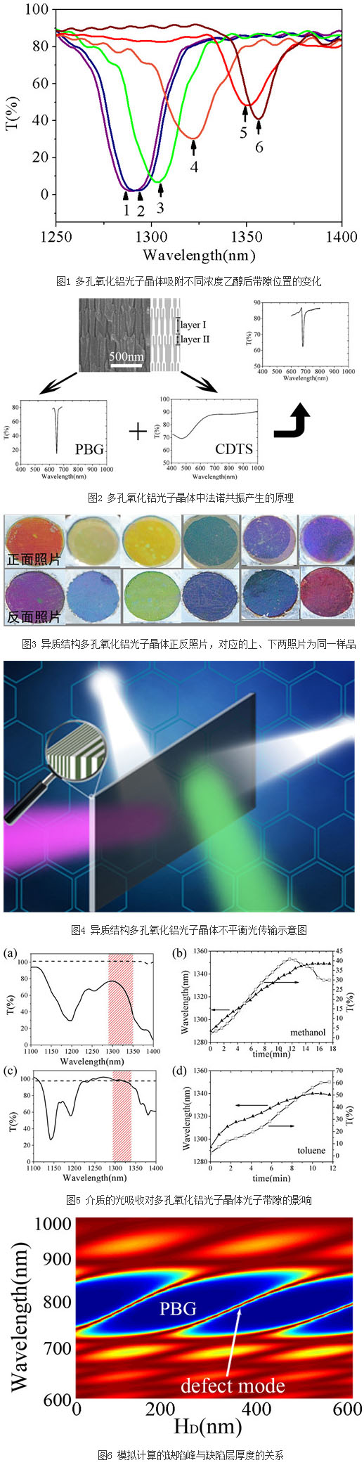
1. ammonium persulfate
Application: Ammonium persulfate is a strong oxidizing agent and can be found in a wide variety of industrial and consumer uses. It appears as a white crystalline powder but may be formulated into cream preparations.
♦ disinfectants and bleaches
♦ bleaching agent for hair colourant and lightener formulations
♦ bleaching and strengthening agent for flour in the baking industry
2. potassium persulfate
This salt is used to initiate polymerziation of various alkenes leading to commercially important polymers such as styrene-butadiene rubber andpolytetrafluoroethylene and related materials.
It is used in organic chemistry as an oxidizing agent, for instance in the Elbs persulfate oxidation of phenols.
As a strong bleaching agent, it is used in hair dye substances as whitening agent with hydrogen peroxide.
It is a Food Additive.
3. sodium persulfate
(1) Used in cleaning and picking of metal surface.
(2) Used in accelerated curing of low formaldehyde adhesives.
(3) Used in modification of starch , production of binders and coating materials.
(4) Desizing agent and bleach activer.
(5) An essential component of bleaching formulations for hair cosmetics.